The ATmega8: An overview
In this post we will learn the basics of AVR ATmega8 micro-controller, which is an AVR series micro-controller unit from Atmel. ATmega8 is the most unexceptional micro-controller for engineering projects. Its simplicity and robustness has made it famous among engineering students. Now-a-days it has become ubiquitous.
In this post we are going to learn how to use basic features of MicroControllerUnit(MCU). In this post, the term ‘MCU’ will refer to the ATMega8 micro-controller.
Architecture of MCU:
ATmega8 is an 8-bit MCU. 8-bit means it can process 8 bits of data per clock cycle. Its data bus has 8 lines. As it is based on CMOS technology, It consumes less power. It is designed on basic of RISC architecture. RISC stands for “REDUCED INSTRUCTION SET COMPUTER”. This is one of the most famous architectures that exist in the world. Another type is CISC which stands for “COMPLEX INSTRUCTION SET COMPUTER”.
• RISC contains very small instruction set.
• RISC contains a large number of general purpose registers for register to register operations which is the reason for fast processing.
• This is a very fast architecture which executes one instruction per clock cycle.
Memory segments of MCU:
This MCU has 8 K byte in-system programmable flash in which we store our programs for execution. We also call it as Program memory. It also has 1Kbyte of SRAM which is also known as Cache memory.
This MCU has 512 Bytes EEPROM for permanent storage of run time data, which will remain saved after turning off the power of the micro-controller.
What is AVR?
The AVR is modified Harvard architecture 8-bit RISC, single chip micro-controller which was developed by Atmel in 1996. The AVR was one of the first micro controller families to use On-chip flash memory for program storage, as opposed to One time programmable ROM used by other micro-controllers at that time.
Atmel says that the name AVR is not an acronym and does not stand for anything in particular. The creator of the AVR give no definite as to what the term ‘AVR’ stands for some users claim that AVR stands for “Advanced Virtual RISC”.
Atmega8:
“Atmega8 is 8-bit micro-controller with 8K Bytes In-system programmable flash”
Advanced RISC architecture
130 powerful instructions-most single clock cycle execution
32 x 8 General Purpose Working Registers
Up to 16 MIPS Throughput at 16 MHz
High Endurance Non-volatile Memory segments
8K Bytes of In-System Self-programmable Flash program memory
512 Bytes EEPROM
1K Byte Internal SRAM
Write/Erase Cycles: 10,000 Flash/100,000 EEPROM
Data retention: 20 years at 85°C/100 years at 25°C
Peripheral Features
Two 8-bit Timer/Counters with Separate Prescaler, one Compare Mode
One 16-bit Timer/Counter with Separate Prescaler, Compare Mode, and Capture
Mode
Three PWM Channels
6-channel ADC in PDIP package
Six Channels 10-bit Accuracy
Byte-oriented Two-wire Serial Interface
Programmable Serial USART
Master/Slave SPI Serial Interface
On-chip Analog Comparator
Special Micro controller Features
Power-on Reset and Programmable Brown-out Detection
Internal Calibrated RC Oscillator
External and Internal Interrupt Sources
I/O and Packages
23 Programmable I/O Lines
28-lead PDIP
Operating Voltages
2.7 – 5.5V (ATmega8L)
4.5 – 5.5V (ATmega8)
Speed Grades
0 – 8 MHz (ATmega8L)
0 – 16 MHz (ATmega8)
Power Consumption at 4 MHz, 3V, 25°C
Active: 3.6 ma
Idle Mode: 1.0 ma
Power-down Mode: 0.5 μA
Now we will see the basic peripheral features.
Input/Output and packages:
This MCU has 23 programmable I/O pins which will be used for interfacing external world. We can configure them as input or output by setting a particular register value, through programming. This IC comes in 3 different packages 28 PIN PDIP, 32 PIN TQFP and 32 PAD QFN/MLF package. Atmega8 is available in two versions: Atmega8 and Atmega8L. Atmega8L is a low frequency version which works on 0-8 MHZ frequency range. There is one more version Atmega8A which is advanced version of atmega8 in the sense of power consumption.
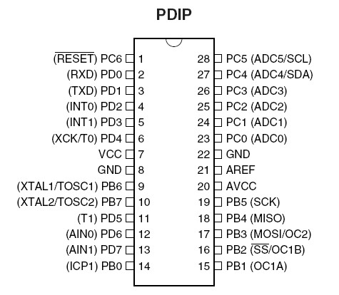
Pin out of atmega8:
Pin description:
VCC
We will be connecting positive terminal of 5 volt regulated supply at this pin.
GND
We will be connecting ground terminal of 5 volt regulated supply at this pin.
Port B (PB7-PB0)
Port B is an 8-bit bi-directional I/O port with internal pull-up resistors (selected for each bit). The
Port B output buffers have symmetrical drive characteristics with both high sink and source capability. As inputs, Port B pins that are externally pulled low will source current if the pull-up resistors are activated. The Port B pins are tri-stated when a reset condition becomes active, even if the clock is not running.
Depending on the clock selection fuse settings, PB6 can be used as input to the inverting Oscillator amplifier and input to the internal clock operating circuit. Depending on the clock selection fuse settings, PB7 can be used as output from the inverting Oscillator amplifier. If the Internal Calibrated RC Oscillator is used as chip clock source, PB7-6 is used as TOSC2-1 input for the Asynchronous Timer/Counter2 if the AS2 bit in ASSR is set.
Port C(PC5-PC0):
Port C is an 7-bit bi-directional I/O port with internal pull-up resistors (selected for each bit). The Port C output buffers have symmetrical drive characteristics with both high sink and source capability. As inputs, Port C pins that are externally pulled low will source current if the pull-up resistors are activated. The Port C pins are tri-stated when a reset condition becomes active, even if the clock is not running.
PC6/RESET:
If the RSTDISBL Fuse is programmed, PC6 is used as an I/O pin. Note that the electrical characteristics of PC6 differ from those of the other pins of Port C. If the RSTDISBL Fuse is unprogrammed, PC6 is used as a Reset input. A low level on this pin for longer than the minimum pulse length will generate a Reset, even if the clock is not running.
Port D (PD7-PD0):
Port D is an 8-bit bi-directional I/O port with internal pull-up resistors (selected for each bit). The Port D output buffers have symmetrical drive characteristics with both high sin and source capability. As inputs, Port D pins that are externally pulled low will source current if the pull-up resistors are activated. The Port D pins are tri-stated when a reset condition becomes active, even if the clock is not running.
AVCC:
AVCC is the supply voltage pin for the A/D Converter, Port C (3..0), and ADC (7..6). It should be externally connected to VCC, even if the ADC is not used. If the ADC is used, it should be connected to VCC through a low-pass filter. Note that Port C (5..4) use digital supply voltage, VCC.
AREF:
AREF is the analog reference pin for the A/D Converter.
As you can see above 23 input/output pins have been divided as PORT B, PORT C and PORT D. In the figure XX, the acronyms written inside the brackets on each pin are an advanced alternate use of that pin. We will discuss them on later posts.
Now let us start using this MCU to interact with real world. This is only possible by using the input pins for taking data into MCU. If we want to send data from MCU to real world we have use the output pins. We can use any port pin as input or output using a register called Data Direction Register (DDR) of that port.
In the first place we must know how this IC works. We know that each and every computer in this world is based on binary system, i.e., 0 and 1. A micro controller is nothing but a small computer which consists of RAM, ALU, control unit, registers, hard disk. So we can consider this MCU as small computer.
We transfer information to MCU in the form of bits and we take information from the MCU in the from of bits. Suppose we have made 4 pins among 23 as input and rest of the pins are output. Now we can program the MCU to show particular bit pattern of 19 bits to those 19 output pins when it receives a special 4 bit number on 4 input pins say “1001”. This can be controlled in programming by checking the input pins and sending a particular data to the particular output pins. But how bits be available on pins of MCU? Yes, right answer is voltage. In TTL and CMOS, 5 V means high voltage which indicates bit 1, and 0 V means low voltage which makes decisions and control something as per that decision. Here, control means controlling the actuators; actuators are nothing but a device or mechanism which can actuate motions, e.g., motors. We can send data available on output pins to anywhere to do some interesting work like starting a motor, starting a fan, starting a robot at remote location, controlling home appliance , etc.
Now we will write a simple program to understand the working of ports. This program will just toggles the output of PORTD. Don’t bother about how to burn this code in to the controller , in coming posts we will discus that.
Blinking LED Project:
//begin

/*
This program will make all leds to blink which are connected to PORTD
*/

#define F_CPU 16000000UL   /*this statement defines the clock speed of MCU(16MHZ in this case)*/
#include<avr/io.h>    //includes input/output header file
#include<util/delay.h>  //includes delay header file

 void wait(int x)
 {
   for(int i=0;i<x;i++)
   _delay_ms(1000); // 1 sec delay
 }

 int main()
 {
    DDRD=0xFF;// PORT D as output port
    while(1)
     {
       PORTD=0b11111111; //all leds are switched on
       wait(1); //wait for 1 second
       PORTD=0b00000000; //sswitch off all leds
       wait(1); //wait for 1 second
     }
  }

//end of program
Program discussion:
In this code, we have defined a macro, F_CPU, in the first line, for specifying clock frequency on which our MCU is working. This macro will be used by the delay function. If clock frequency is not defined in our program some default value will be taken automatically which is defined in ‘delay.h’ header file.
In the next line we have included a header file for using some ready made functions and keywords.
In the third line we have included another file for creating the delay. The function exists in the ‘util’ folder in default inclusion directory.
After starting the main function, our first line is DDRD=0XFF; which is used for defining the data direction line of I/O pins. This means that all the 8 pins of PORTD will become output PINs. So MCU will send data on these pins, which in turn will send to the external world. Storing bit 1 in DDRD register’s particular bit will make it’s corresponding pin as output pin and storing 0 will make it’s corresponding pin as input. Remember that DDRD is an 8 bit register capable of storing 8 bits of data which defines the data direction. If we connect 8 LED’s on the 8 pins of PORTD and if the data on these pins are all 1, then all LED’s will glow.
Similarly we can make all pins as input by writing these this code:
DDRD=0x00;
DDRD is an 8 bit register for setting data direction line of PORTD. Similarly we have DDRB and DDRC. We can set a particular pin as input or output by setting it’s corresponding bit as 0 or 1 respectively. If want to set/reset a particular bit of a register you can use the following statements.
DDRD|=(1<<PD4); // this statement will set the PD4 bit
DDRD &=~(1<<PD4); // this statement will reset the PD4 bit
Now we have started an infinite loop for continuous blinking.
After that we will send the on PORTD as high on all 8 pins by command PORTD=0Xff;
Similarly we can send data 0, on all 8 pins by command PORTD=0x00;
Now all we need to do is to insert some delay between these two commands so that we see the LED’s blinking otherwise they fill blink at such a rapid speed that our eyes will see a continuous glow rather that blinking LED’s.
We have used a wait function for inserting some delay can be varied.
Use the function like this:
Wait(2);
This means you are creating a delay of 2 sec. you may run your MCU on internal/external clock generators. Until unless you write fuse bits for the external crystal oscillator, MCU will not use the external oscillator. By default MCU runs on 1 MHz calibrated internal RC oscillator.